
In This Article
What is Architecture of Central Processing Unit?
CPU architecture refers to the layout of all the components that make the unit. Technically, CPU architecture has two parts namely the Instruction Set Architecture or ISA and the microarchitecture.
In simple terms, CPU architecture signifies the arrangement of the components which include the Arithmetic Logic Unit, the Control Unit, different registers and buses.
KEY TAKEAWAYS
- The ALU of the CPU does all the arithmetic and logical calculations and all these are overseen by the Control Unit.
- The different registers in the CPU perform different basic functions such as storing the calculation results, data address, processed data and address of following instructions.
- Most modern CPU architectures are based on von Neumann but there are also a few that are based on the Harvard architecture.
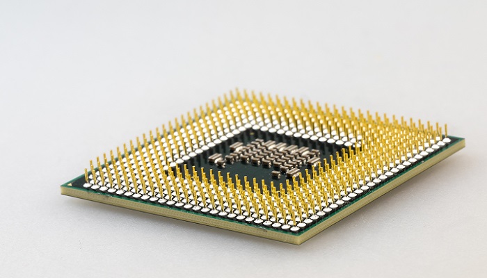
- Transistors are usually used today to build CPUs that makes the architecture more complex but enables building it on one or more PCBs.
Understanding Architecture of Central Processing Unit
The CPU or the Central Processing Unit of a computer is actually an electric circuitry. This helps it in carrying out several instructions given to it by a computer program.
The CPU is known by different names such as:
- A central processor
- The main processor or simply as
- A processor.
However, the CPU is the backbone of a computer performing several functions which comprise basic arithmetic functions, logical functions, as well as controlling the functions of other components including and I/O operations.
If you want to know about the CPU architecture and visit different websites or even read books on computer, you will be presented with a block diagram of it which will consist of three major units namely:
- The memory or storage unit
- The control unit and the
- Arithmetic Logic Unit or ALU.
However, the architecture of the CPU was neither as simple as it was before nor as it is now.
Apart from the main components of a CPU mentioned above, there are also several other elements that help it perform in the best possible way.
It includes processor registers which helps the ALU in its operation by supplying the necessary operands to it and storing the results of its operations.
The control unit orchestrates all functions of the ALU such as fetching data from the memory, decoding them and executing the instructions.
The memory or storage unit of the CPU stores all data and instructions, intermediate or final, just as the name signifies.
However, the memory unit also transfers information to other units when needed.
Ideally, the structure of the memory unit of a CPU consists of two specific types. These are primary memory and secondary memory.
The control unit of the CPU, as the name suggests, controls the operations of every part of it but it does not perform data processing operation itself.
It simply uses the electrical signals to instruct the computer. The instructions are sent by the memory unit which the control unit decodes before execution.
The primary job of the control unit is to ensure that the flow of instructions across the computer is maintained.
And, the Arithmetic Logic Unit does all the arithmetic and logical calculations.
The arithmetic operations such as addition, subtraction, multiplication, and division, are done in the arithmetic section of the ALU and the logical operations such as selecting, matching, comparing, and merging the data, are done in the logic section.
Apart from these three basic parts that are often discussed, there are also other parts of a CPU such as the registers. These are those parts of the CPU that store data.
The registers typically operate like the RAM but the memory cells in it consist of logic gates rather than capacitors.
The registers can perform much faster than RAM but cannot store as much data as a RAM can.
Within the CPU architecture, there are five different types of registers. Here they are with their basic functions:
- Accumulator – It stores the calculation results
- Instruction Register – It stores the address in RAM of the instruction needed to be processed
- Memory Address Register – It stores the data address in RAM that is needed to be processed
- Memory Data Register – It stores the data which is processed and
- Program Counter – It stores the address of the subsequent instruction in RAM.
Now, with the development of technology, modern CPU architecture consists of IC or Integrated Circuit microprocessors.
A single IC chip may contain one or more CPUs. Therefore, these chips are also called multi-core processors. The IC chip contains everything that is needed by a CPU such as:
- The memory
- The peripheral interfaces and others.
Quite rightfully these microprocessors are called the microcontrollers or System on a Chip or SoC.
Moreover, the processor cores which act as individual physical CPUs are now multithreaded as well. This helps in creating additional logical or virtual CPUs.
Then there are the vector processors or array processors that come with a different architecture altogether.
These come with multiple processors that function in parallel. This means that no specific unit in it is considered to be the central processor.
Now, with so many different variants, it is paramount that you dive deeper and take a closer look at the architecture of the Central Processing Units, along with its history and evolution.
Architecture
The construction of Central processing Units of the computers in its early days was very huge and cumbersome for which these computers, such as the ENIAC and others, were referred to as ‘fixed program computers.’
These needed to be rewired physically to carry out different tasks.
The term “Central Processing Unit’ has been in use since 1955 and was usually defined as a tool for executing software or computer programs.
However, the earliest tool that can be termed a CPU rightfully came after the arrival of the stored program computer.
The main idea of the stored program computer was already present in the ENIAC designed by J. Presper Eckert and John William Mauchly. However, in order to finish it soon, this idea was omitted initially.
The First Draft of a Report on the EDVAC, a paper distributed by mathematician John von Neumann on June 30, 1945 is however considered to be the outline of the stored program computers and was completed in August 1949.
The EDVAC could perform a specific number of operations of varied types but the programs written for it needed to be stored in a memory of high speed in the computer instead of that specified by the physical wiring.
This was the serious limitation of the ENIAC since it needed a huge amount of time and effort to reconfigure so that it could carry out a new task. With the design of EDVAC it could be changed easily by changing the memory contents.
The architecture of the early CPUs was used for larger computers, and sometimes for specific computers.
This is why these CPU architectures had custom designs. However, this did not offer a chance to produce multipurpose processors in large quantities.
Therefore, it needed standardization which gave rise to the era of minicomputers and distinct transistor mainframes.
This trend gained popularity and accelerated rapidly with the advent and popularization of ICs.
These ICs allowed designing more complex CPUs with varied tolerance levels depending on the order of the nanometers.
With the standardization and miniaturization of the architecture of the CPUs, the modern computers now have much more utility than the dedicated computers of the yesteryears.
The design of the stored program computers came to be known as the von Neumann architecture.
However, different concepts such as that of Konrad Zuse were implemented in the purported Harvard architecture of the Harvard Mark I.
It was completed even before EDVAC and used punched paper tape instead of electronic memory.
The main difference between the von Neumann architecture and the Harvard architectures is that the latter separates the treatment and storage of CPU data and instructions as opposed to the same memory space used by the former.
The architecture of most modern CPUs is mainly based on von Neumann but you will get CPUs with the Harvard architecture as well.
These are typically used in embedded applications.
The functioning and level of performance of a CPU also depends on the thermionic vacuum tubes and relays.
These are usually used as switching elements and a computer needs thousands or tens of thousands of them to be useful.
The speed of these switches eventually determines the overall speed of the system.
In the olden days, the vacuum tube based EDVAC computers and others could operate for about 8 hours before failing but the Harvard Mark I, which is a slower computer but had relays, seldom failed.
However, the tube based computers dominated the scene due to their higher speed of operations and greater reliability. These computers comparatively ran at a much lower clock rate.
Now, take a look at the different types of CPUs based on their different architecture and components used.
Transistor CPUs:
Over time, the need for building smaller yet more reliable computers pushed the designers to use different technologies.
The first notable improvement in the design of the CPU was the arrival and use of transistors.
CPUs using a transistor did not need to use those unreliable, bulky and fragile switching elements such as the relays and vacuum tubes.
This significant development paved the way for more reliable yet more complex CPU architecture.
The CPU architecture now could be built on one or more PCBs or Printed Circuit Boards.
Small Scale Integration or SSI CPUs:
Then after, interconnected transistors were designed and manufactured in a more compact space.
These were called the ICs or Integrated Circuits used to build the CPUs. The ICs allowed manufacturing more transistors on only one chip.
This chip is a semiconductor-based die. Initially, NOR gates or other non-specialized and very basic digital circuits were miniaturized into the ICs and were considered as the building blocks of SSI or Small Scale Integration devices.
Irrespective of being small and integrated, these ICs normally came with up to a couple of dozen transistors and thousands of such chips were needed to build a CPU.
However, these CPUs consumed much less power and space in comparison to the discrete, traditional transistor architecture of the earlier days.
Large Scale Integration or LSI CPUs:
Then, it was the Large Scale Integration or LSI circuits that were built which included more than a hundred gates.
These were built by using the MOS or Metal Oxide Semiconductor process.
However, these chips were slower and were useful only in those particular applications that needed low power.
Hence companies still continued to build bipolar TTL chips.
The design was further developed in 1968 by using silicon-gate MOS technology by Federico Faggin.
These chips replaced the bipolar TTL or Transistor-Transistor Logic as standard chip technology in the 1970s.
Microprocessors:
The first commercially available microprocessor was available in 1971 in the form of Intel 4004. However, the first microprocessor that was used widely was Intel 8080 that was launched in 1974.
This particular class of CPUs took over all other CPU architectures and was so dominant that mainframe and minicomputer manufacturers introduced proprietary IC development programs.
This allowed them to upgrade old computer architectures.
This resulted in the further development of instruction set compatible microprocessors. These chips were backward compatible and therefore can be used with older hardware and software.
The success of the microprocessors was so grand and combined with the advent of the personal computers, these chips became omnipresent in the CPU architecture.
Several CPUs or cores can be integrated on one single chip which makes the CPUs perform much faster and better.
With such developments in the chips and their implementation in the construction, the architecture of the modern is made more compact, useful, and productive.
Based on the set of basic operations hardwired into the electric circuitry of a CPU, it performs several functions.
These instructions consist of a unique arrangement of bits called the machine language opcode.
The CPU uses a binary decoder to decode this opcode into control signals. This controls the behavior and operations of the CPU.
Here, the architecture of the CPU comes in. All mathematical operations are carried out in the ALU which is actually a combination of logic circuits.
It fetches instructions from the memory, as said earlier, and stores the result.
Along with other functions, the CPU also carries out mathematical operations on floating-point numbers in the floating-point unit.
The control unit is the next important part of the CPU architecture which directs the operations of the processor.
It directs the flow of data between the CPU, memory, ALU, input and output devices by providing control and timing signals.
In modern computers, the control unit forms an integral part, a component that was included by John von Neumann in the von Neumann architecture.
The next important part of the CPU architecture is the Address Generation Unit or AGU, which is also called the Address Computation Unit or ACU sometimes.
This is basically an execution unit found inside the CPU. The main job of it is to addresses that are used by the CPU to access the main memory for fetching data.
Including an AGU in the CPU architecture lowers the number of CPU cycles significantly for executing different machine instructions.
This improves the overall performance of the CPU. It works parallel to the CPU which takes away a significant amount of load from the CPU.
Some specific CPU architectures come with multiple AGUs as well. This enables them to execute more than one address calculation operation simultaneously.
This improves the performance of the CPUs by making the most out of the advanced, superscalar design.
A Memory Management Unit or MMU is also included in the PU design nowadays, especially in those that are used in smaller computers such as desktops, laptops, smartphones, apart from the server computers.
This particular unit helps in interpreting logical addresses into physical memory addresses.
It also protects the memory and provides paging abilities which is very helpful for virtual memory. However, microcontrollers and other simpler processors do not come with an MMU.
There are also a few other smaller yet important parts included in the CPU architecture as mentioned below.
Cache:
There is a hardware cache in the Central Processing Unit of a computer. This reduces the average cost of time and energy while accessing data from the main memory.
It is actually a much smaller but faster memory which is closer to the core of the processor.
It stores copies of different data and information that are used often from the primary memory locations.
All modern CPUs that are fast and specialized come with multiple levels of caches.
Most CPUs have different independent caches and are organized typically as a hierarchy such as Level 1, Level 2, and Level 3 and so on.
In the older CPUs, there was only one level of cache and it did not have any separate part for data and instructions.
However, the modern Level 1 caches come with two divisions namely L1d for storing data and L1i for storing instructions.
Larger processors come with more caches marked Level 2 and Level 3 where the L2 cache acts as a common repository for the already split L1 cache and is normally not split.
In a multi core processor, every core has a dedicated Level 2 cache and therefore is not shared among the cores.
The Level 3 cache, on the other hand, along with other higher level caches, is usually not split and is shared among the cores.
As for the Level 4 caches these are quite uncommon and are usually found in DRAM or Dynamic Random Access Memory instead of in a Static Random Access Memory or SRAM. The TLB or Translation Look-aside Buffer is a part of the MMU.
Every higher level of cache is usually bigger and can be optimized in a different way. Typically, caches come in powers of 2, 8, 16 or higher KB or MB.
Clock Rate:
The CPUs typically function as a synchronous circuit. This means that the CPUs expedite their sequential operations by using clock signals.
These signals are generated by an exterior oscillator circuit. This circuit sends a constant number of pulses every second.
These form a periodic square wave.
The rate at which the CPU can execute an instruction is determined by the rate of recurrence of the clock pulses.
This means that more instructions will be executed by the CPU every second if the clock is faster.
However, the clock period is deliberately set longer than the highest time taken by all the signals to propagate through the CPU.
This prevents issues related to worst-case movement delay.
This simplifies the CPU from both the component count and design point of view. But, there is a disadvantage.
The CPU has to wait on the slowest elements. This can be overcome by increasing the parallelism of the CPU, which is discussed later in detail.
Also, there is an issue regarding the delays of other electrical signals which architectural improvements alone cannot solve completely.
If the CPU is more complex, it is more difficult to maintain a proper synchronization of the clock signal all through the unit.
This will need several identical clock signals in the CPUs to avoid the CPU from malfunctioning due to the delay of a single signal.
Also, when the clock rate increases significantly, a considerable amount of heat is dissipated by the CPU.
This is because the constantly changing clock makes several components in the CPU to switch even if these are not used.
As a result, it consumes more energy needing the CPU to dissipate more heat.
Clock gating is one proven way to overcome this issue which will prevent switching of the unneeded components.
In this process, the clock signal is turned off, disabling the unneeded components.
However, this can only be implemented in low-power designs because it is difficult to implement.
This resulted in designing asynchronous CPUs or clockless CPUs which remove the clock signal altogether.
Though this is complex, it offers significant advantages especially in the case of power consumption and heat dissipation.
To make things less complicated, instead of removing the global clock signal completely, some CPUs are designed with a few specific asynchronous portions in it such as the ALU with superscalar pipelining.
Voltage Regulator:
There are several modern CPUs that have a die-integrated power managing or voltage regulator module included in their design.
This helps in controlling the demand of voltage supply to the electrical circuitry of the CPU.
As a result a proper balance between power consumption and performance of the CPU is maintained.
Integer Range:
The CPUs represent numerical values in a definite way. While some early ones represent them as a familiar decimal or base 10 numeral system values, others use unusual ways such as base three or ternary numeral systems to represent the numbers.
However, most of the CPUs these days follow the binary form to represent the numbers where each of them is represented by a two-valued physical quantity.
These devices use word sizes that are typically a power of two – 8, 16, 32 or 64 bits.
The size and accuracy of the numbers represented by a CPU is related to the numeric representation.
In binary form, it is calculated by the amount of bits processed by the CPU in a single operation.
This is called in different ways such as word size, integer size, bit width, integer precision, or data path width.
The integer size of the CPU determines the integer range that it can operate directly.
This integer range also affects the number of memory locations that can be addressed by the CPU directly.
This can be a serious imitation in some cases which is why some CPUs use specific mechanisms such as bank switching.
This allows adding additional memory that is to be addressed.
However, this may not solve issues related to higher or lower bit lengths which is why different bit widths are used by several instruction sets for floating point and integer data.
This allows the CPUs to have varied bit widths by using the instruction set for different parts of the device.
Several CPU architectures used this mixed bit width concept in their design which helped the processors to be used for general purpose where it is necessary to have a reasonable balance between the integer and floating point capabilities.
Parallelism:
The modern CPU architecture solves the limitations in performance by the subscalar CPUs of being able to execute and operate on one instruction on one or a couple of data at a time which is less than 1 IPC or Instruction Per Clock Cycle.
The subscalar CPUs often had to wait for the completion of one instruction to start a new one. As a result, these CPUs got ‘hung up.’
The performance is therefore affected and cannot be improved even if a second unit is added to it. In fact, it made the situation worse.
Now, instead of one, two pathways get hung up. This results in the increase in the number of unused transistors.
One of the significant changes in the design methodologies and CPU architecture is to make them work in parallel. This is done in two specific ways such as:
- Instruction-level parallelism – Often referred to as ILP, in this process the rate of execution of instruction is increased within the CPU with an increased use of the on-die execution resources and
- Task-level parallelism – Referred to as TLP, in this process increases the processes or threads that the CPU can execute at the same time.
Both these methods differ in the ways of implementation and their comparative effectiveness in increasing the performance of the CPU for an application.
Data parallelism is however a less common but an important paradigm of processors. Unlike the scalar processors, the vector devices deal with several pieces of data in one instruction.
This is referred to as SIMD or Single Instruction Stream, Multiple Data Stream as opposed to SISD or Single Instruction Stream, Single Data Stream in the scalar processors, according to Flynn’s taxonomy.
Nowadays, processors are designed to handle vectors of data which helps in optimizing performance and time taken to complete an operation even when it is required to process a large set of data.
These vector processors can fetch, decode, and execute an instruction at one go.
The design of the vector processors have changed significantly from their early variants that were used mainly for cryptography applications and scientific research.
Now, with multimedia shifting to digital media, the need of SIMD is more significant.
Therefore, incorporation of SIMD execution units is seen now in the processors used for general purpose especially after the addition of floating-point units.
However, some of the initial SIMD specifications were integer-only which turned out to be a serious hindrance for the software developers.
This is because most of the applications that gained from SIMD typically handle floating-point numbers.
Therefore, the developers remade and refined the initial designs little by little changing them into a more modern and more effective SIMD specifications.
These are typically related to one ISA or Instruction Set Architecture.
Hardware Performance Counters:
There are several modern architectures which include the embedded ones that come with an HPC or a Hardware Performance Counter.
This allows low-level collection, debugging, benchmarking, or analysis of the metrics of the running software.
These counters also help in finding out and analyzing any suspicious or unusual activity of the software such as Return Oriented Programming or ROP and SROP or Sigreturn Oriented Programming.
This is very helpful for the software developers and the security teams for finding out and assessing malicious binary programs.
Virtual CPUs:
And finally, now with cloud computing in vogue, it is needed to subdivide the operations of CPUs into virtual processing units.
In this particular design, there is a host computer or server that acts as a virtual physical machine. The entire virtual system works on this machine.
When a number of physical machines operate in tandem and are controlled as a single unit, it forms a cluster of memory resources and allows group computing.
There are several systems in which it is possible to add or remove a cluster dynamically and the resources that are available at the host computer and at the cluster level can be divided into resource pools with superior granularity.
Formats
Every instruction within the computer is represented by a series of bits which follows a specific format or way of expression.
The bits are divided into different groups called fields.
The instruction format can be of different types and each of these formats is typically characterized by a rectangular box. These are:
- Variable Instruction Formats – The lengths of these particular instructions vary on the basis of the op-code and address specifiers. Such instructions usually have a good code density but these are very difficult to pipeline or decode.
- Fixed Instruction Formats – All such instruction formats are of the same size. Quite naturally, these formats are quite easy to decode and pipeline but they do not have a good code density.
- Hybrid Instruction Formats – These formats come with varied lengths. These are specified by the opcode. Being hybrid in nature, these formats usually have the benefits of both the above mentioned formats.
In the end, the gist of the matter is that the architecture of a CPU has changed significantly over time in its design, form, and implementations.
However, the basic operations of it have remained almost unchanged – to process a given set of instructions as quickly and correctly as possible.
Conclusion
The computers now are more advanced yet smaller than before.
Going through this article, now you surely know what your CPU is made up of and how things have changed over time.