")
In This Article
What is Communication and Network Riser (CNR)?
CNR, short for Communication and Network Riser, refers to the specification for different interfaces such as modem, audio, LAN and USB found in the core logic chipsets.
This technology was developed and introduced by Intel especially for the motherboards belonging to the ATX or Advanced Technology Extended family.
KEY TAKEAWAYS
- The Communications and Networking Riser card was developed by Intel on February 7, 2000 to be used in the Advanced Technology Extended family of motherboards.
- This riser card is used for varied purposes such as in specialized audio, networking, and telephony equipment.
- The design of the CNR allowed the motherboard manufacturers to save on the production costs by doing away with the analog I/O parts from the board.
- These riser cards were extensively used on the Pentium 4 motherboards for several years but were slowly overshadowed by different embedded or on-board components such as the Peripheral Component Interconnect Express or PCIe.
Understanding Communication and Network Riser (CNR)
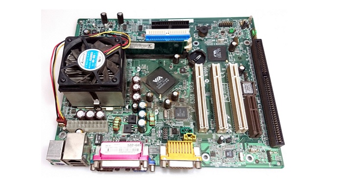
Communications and Networking Riser is the slot integrated on some of the computer motherboards.
The design of these riser cards allows offering different types of functionality in the specialized audio, networking, and telephony devices irrespective of the combination on the CNR card.
This particular interface was developed by Intel with the main intention to replace their previous Audio Modem Riser cards.
These new cards offered two notable advantages over the earlier AMR cards such as:
- Capability of being controlled by software or CPU and hardware accelerated as with a dedicated ASIC or Application Specific Integrated Circuit and
- Plug and Play feature.
As for the design, a few motherboards had the last PCI slot replaced by the CNR slot but in most of the cases the motherboard were engineered in such a way that it allowed the manufacturers to introduce the CNR that would share the same space as the last PCI slot.
Physically, the CNR slots consist of two rows of 30 pins. Based on their configuration these slots were classified into two specific heads such as:
- Type A and
- Type B with separate pin assignments.
There is the characteristic 8-pin PHY or Physical Layer interface in Type A CNR but, in comparison, the Type B CNR comes with a 17-pin MII or Media Independent Interface bus Local Area network or LAN interface.
However, both these types of CNRs are able to carry both AC 97 or Audio Codec 97 and USB or Universal Serial Bus signals.
The design, features and functionalities of the CNR as compared with the AMR offered significant cost saving potential to the manufacturers primarily because it allowed removing the analog I/O elements from the motherboard.
This, in turn, allowed the manufacturers to abide by the requirements of the US Federal Communications Commission or FCC certification for the CNR cards only and not of the whole motherboard.
This means that they could now avail a much quicker production to market time for the new motherboards.
This eventually led to mass production of CNR cards for use in several motherboards.
On the whole, the CNR cards helped the Original Equipment Manufacturers or OEMs to lower the cost manufacturing different subsystems such as:
- LAN
- Audio
- Home networking and
- Modem.
As for the specification of the CNR, it is typically an open industry specification that defines a scalable interface and a motherboard riser card.
In addition to that, the specification also defines the specific architecture of the CNR for both regular as well as low profile riser cards and includes different aspects of the riser interface such as:
- Mechanical
- Electrical and
- Thermal requirements.
This specification is supported by Microsoft, different silicon suppliers as well as a variety of OEMs.
The main reason for the CNR to gain such widespread support is that it conforms to the current technologies such as Ethernet, analog modems and others.
Also, this particular technology supported expanding it for other developing technologies such as Digital Subscriber Line or DSL. The CNR bus however does not support an expansion slot.
The specification of CNR also defines the size of the board and the pin-out configuration according to it.
Here are the pin-out configurations of the Type A and Type B CNR for you.
The Type A CNR pin-out is as follows:
- Pin 1, Pin 2, and Pin 5 on both side A and B are reserved
- Pin 3 and Pin 6 on side A is for ground and on side B is reserved
- Pin 4 is just the opposite of Pin 3 where that of side A is reserved and of side B is ground pin
- Pin 7 on side B is for ground and on side A for LAN_TXD2
- Pin 8 on side B is for LAN_TXD1 and on side A for LAN_TXD0
- Pin 9 on side B is for LAN_RSTSYNC and on side A is for ground
- Pin 10 on side B is for ground GND and on side A is for LAN_CLK
- Pin 11 on side B is for LAN_RXD2 and on side A is for LAN_RXD1
- Pin 12 on side B is for LAN_RXD0 and on side A is reserved
- Pin 13 on side B is for ground and on side a is for USB+
- Pin 14 on side B is reserved while that on side a is for ground
- Pin 15 on side B is for +5 volt dual and on side A is for USB –
- Pin 16 on side B is for USB_OC# and on side a is for +12 volts
- Pin 17 on both sides are for ground
- Pin 18 on side B is for -12 volts and on side A is for +3.3 volts dual
- Pin19 on side B is for +3.3 volts and on side A is for +5 volts
- Pin 20 is followed by two keys and it is for ground on both sides
- Pin 21 on side B is for EE_DOUT and on side A is for EE_DIN
- Pin 22 on side B is for EE_SHCLK and on side A is for EE_CS
- Pin 23 on side B is for GND and on side A is for SMB_A1
- Pin 24 on side B is for SMB_A0 and on side A is for SMB_A2
- Pin 25 on side B is for SMB_SCL and on side A is for SMB_SDA
- Pin 26 on side B is for CDC_DN_ENAB# and on side A is for AC97_RESET#
- Pin 27 on side B is for GND and on side A is reserved
- Pin 28 on side B is for AC97_SYNC and on side A is for AC97_SDATA_IN1
- Pin 29 on side B is for AC97_SDATA_OUT and on side A is for AC97_SDATA_IN0 and
- Pin 30 on side B is for AC97_BITCLK and on side A is for GND.
On the other hand, the Type B CNR pin-out is as follows:
- Pin 1 on side B is for MIL_MDIO and on side A is for MIL_MDC
- Pin 2 on side B is for MIL_COL and on side A is for MIL_CRS
- Pin 3 on side B is for MIL_TXC and on side A is for GND
- Pin 4 on side B is for GND and on side A is for MIL_RXDV
- Pin 5 on side B is for MIL_RXERR and on side A is for MIL_RXC
- Pin 6 on side B is for MIL_TXD3 and on side A is for GND
- Pin 7 on side B is for GND and on side A is for MIL_TXD2
- Pin 8 on side B is for MIL_TXD1 and on side A is for MIL_TXD0
- Pin 9 on side B is for MIL_TXEN and on side A is for GND
- Pin 10 on side B is for GND and on side A is reserved
- Pin 11 on side B is for MIL_RXD2 and on side A is for MIL_RXD1 and
- Pin 12 on side B is for MIL_RXD0 and on side A is for MIL_RXD3.
The functions of Pin 13 to Pin 30 of Type B CNR are the same as that of the Type A CNR.
With all this said, it is good to add that the CNR is not used today as it was found in the old Pentium III motherboards due to the integration of better components such as Ethernet, PCIe, and audio into it.
CNR Functions
The main function of the CNR is to integrate the Ethernet based Local Area Networks, broadband and multichannel audio and analog modem subsystems with the personal computers.
It functions in a specific way which involves:
- Minimizing the electrical noise interference
- Separating the elements sensitive to noise physically and
- Enhancing the overall communication system of the motherboard.
Most importantly, it removes the need for the analog I/O components which reduces the manufacturing costs of the motherboards as well.
Conclusion
This article has tried best to keep you informed about the Communications and Network Riser card and slots, which, however, is replaced by better on-board elements.
You now know about its functions, pin-out configuration and why it was used extensively in the older motherboards and other subsystems.