What is FinFET (Fin Field Effect Transistor)?
Fin Field Effect Transistor or FinFET in short, refers to a 3D or non-planar transistor mainly used to make those modern processors. From the point of view of its architecture, it is built on SOI substrate as it was in the earlier planar designs.
However, technically, these transistors have a separate conducting channel rising above the insulator. This is the gate electrode. It is the fin-shaped and thin silicon structure that allows several gates to operate on one single transistor.
Understanding FinFET (Fin Field Effect Transistor)
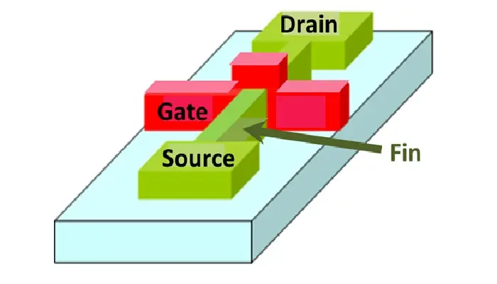
A Fin Field Effect Transistor is a multi-gate device and is easily distinguishable due to the source and drain terminals that look like fins on the silicon structure.
It is actually the fin projections that are the source and drain channels that are wrapped by the gates.
These transistors usually are better than the planar CMOS or Complementary Metal-Oxide Semiconductor technology because:
- They have quicker switching times
- They offer better current density.
These transistors have now become the foundation for the fabrication of the nano-electronic semiconductor devices and microchips with gate designs at 14 nm, 10 nm and 7 nm process nodes.
There are several fins on a single FinFET transistor set side by side. All these fins act as one electrically and are covered by the same gate. This has dual benefits such as:
- It enhances the performance
- It increases the drive strength.
This technology extends Moore’s law and allows the manufacturers to design semiconductors to build smaller memory modules and CPUs that consume less energy but work faster.
Invented by Chenming Hu, Tsu-Jae King-Liu, and Jeffrey Bokor at the University of California, Berkeley, the fins of FinFETs not only form the source and drain terminals but also offer a higher volume in a small area at the same time.
The gates surrounding these fins offer greater control over these channels reducing the chances of any leakage through the body in the ‘off’ state.
It also allows lowering the threshold voltage. This, in turn, helps in two specific ways, such as:
- It reduces power dissipation
- It increases performance.
The orientation of these gates is at right angles to the vertical fins and the wrapping enables them to interface with three sides of the channel.
This ensures better electrical control over the conductivity of the channel and also diminishes short-channel effects.
The use of FinFETs has enabled the industry to handle leakage current more effectively, especially today when the transistors have become smaller. This is mainly due to the wrap-around structure.
This unique design helps in the following ways:
- It reduces the short-channel effects because the gate needs to deal with different operation modes which help in making the electric field within the channel more uniform.
- It also eliminates doping variations within the body and thereby lowers the threshold voltage variations due to the body effect or substrate bias.
- It allows adapting the same processing steps as CMOS for its fabrication in spite of being non-planar.
- It allows further scaling on new parameters beyond planar architecture due to fin height, thickness, and gate length. If the gate length is more than the fin thickness, leakage current can be suppressed better.
Read Also: What is Amber Lake Processor? (Explained)
It is all due to the geometry of these transistors and the raised channel regions on the substrate that they offer such benefits.
What is FinFET Used for?
FinFET is used as a switch and as an amplifier in several applications such as computers, smartphones, wearables, tablets, automotive, high-end networks and more.
The different advantages offered by the FinFETs also allow them to be used for other specific applications such as:
- It helps in designing RAM or Random Access Memory modules due to the low current in the off state.
- It helps in designing power amplifiers and other analog circuits that need a superior quantity of linearity.
The tri-gate structure of these transistors also allowed them to be used in 5 nm and 7 nm CMOS devices.
What is Fin in FinFET Technology?
The fin actually refers to the structure of the FinFETs that typically resembles the dorsal fins of a fish. The FET structure looks just like a set of fins, and hence the name.
These three-dimensional bars or fins made of silicon are the main body of the transistor that distinguishes it from the others and, as said earlier, also form the source and the drain offering more volume in a small area.
How Does FinFET Reduce Leakage?
Typically, these transistors come with channels or fins that are fully wrapped at the three sides with the gate. It is this gate design as well as the FET, which refers to the field-effect caused by the electric field created, that offers a much better control over the conductivity of the substance.
This makes them highly depleted channels which eventually help in reducing leakage.
Actually, the design of the FinFETs facilitates the following:
- Lowering the leakage power to half
- Reducing the dynamic power.
The multiple gates of the FinFET surrounding the thin fins reduce the charge carriers which offer better current flow within the channel and electrostatic control.
This prevents leakage of current during an ‘off’ state between the source and the drain.
Also, the smaller geometries of the FinFETs offer higher variability which allows them to operate at a lower voltage.
This also helps in reducing leakage eventually, much contrary to the common concept that lowering threshold voltage results in increased leakage.
Is FinFET a Transistor?
Yes, just as the full form of it implies, a FinFET is a transistor that is designed to overcome the short-channel effects that are commonly encountered by transistors in order to attain higher performance metrics at a lesser cost.
How Does Current Flow in FinFET?
The tall and thin fins of the channels that are lifted off the insulating substrate have the source and drain at both ends and the three gates are close to the top and their sidewalls.
The current actually flows through these channels or fins from the source, and its flow is controlled by the gates.
Typically, the FinFETs follow width linearization by designing the width as the multiples of height.
This height is the main aspect that allows and controls the current flow through the sources and the drain.
The higher the height, the more will be the current flow through the channel.
Other aspects of the design of the transistors also help in current flow through the channels and managing it. These are as follows:
- The fins enhance the gate area that surrounds the channel and reinforce its control over the channel and the flow of current through it.
- The design also reduces the short-channel effect more effectively, which, in turn, reduces leakage current, increases circuit control, and shortens gate length, all of which facilitate and control current flow.
- Since the channels are not doped, the effects due to the scattered impurity ions are also reduced effectively. This increases the mobility of the channel carrier and influences the flow of current.
And, the wrap-around gate offers low threshold voltage, which reduces power dissipation and increases the performance to eventually help in the current flow.
What are the Types of FinFET?
FinFETs can be categorized into two major groups, namely, single gate structure, and double gate structure. However, based on the gate structure and other features, there can be other sub-divisions such as Shorted Gate or SG FinFET, Independent Gate or IG FinFET, and more.
SG FinFET:
These specific transistors have three terminal devices, physically connected front gate and back gate, and higher ON current and OFF current. The two gates control the electrostatics of the channel.
IG FinFET:
These transistors have four terminal devices, physically isolated front and back gates, and usually do not provide a larger space area due to the two different gate terminals.
However, the isolated gates allow applying different voltages to them which is very useful. This flexibility allows linearly modulating the threshold voltage of the front gate with the help of the back gate bias.
In addition to the above, there are also other types of FinFETs that come with different substrate types, electrical characteristics, number of gates and structures and channel directions.
For example, based on the substrate, there are two types of FinFETs namely, SOI FinFET and the bulk FinFET. They both have similar parasitic capacitance and resistance and offer the same power performance at the circuit level.
SOI FinFET:
The Silicon on Insulator transistors are made up of a substrate that has a lower thermal conductivity which is due to the masked oxygen layer in it.
These light fin doped transistors offer higher mobility, lower junction capacitance and higher electrical performance due to their voltage gain.
Bulk FinFET:
These are built on bulk silicon substrate and with a different process. This offers lower defect density, lower cost, and better heat dissipation performance.
Why was FinFET Invented?
The primary reason to create FinFETs is to have better channel control and a better current flow through it. Add to that, the more area offered by the thinner fins allow the designers to fit in more components on a single chip.
Also, the companies wanted something that was easier to implement to manufacture smaller ICs.
Another significant reason for creating the FinFETs is to conform to Moore’s Law.
This law states that the number of transistors will double on a computer chip every 18 to 24 months to create more powerful electronic devices and meet higher computing demands.
How is FinFET Made?
The most significant and distinguishing feature in the making of the FinFET is designing the channels or fins that stay above the surface. It is made from silicon and contains gates that wrap the channels from all three sides instead of just the top.
Ideally, the FinFETs are made in unique way as follows:
- It has a 3D geometry that allows further scaling.
- The transistors are positioned vertically which allows for shrinking the dimensions and packing more components onto the silicon chip.
- The heights of the fins are increased which consumes less room on the die but allows a higher flow of current.
- The structure of the fins is made according to the leading-edge technologies of today such as Self Aligned Double Patterning or SADP and Self Aligned Quadruple Patterning or SAQP.
All these methods followed in the making of the FinFETs increase the eventual performance of the device.
What is the Threshold Voltage of FinFET?
Ideally, the FinFETs with the lowest doping concentration have only one threshold voltage at a single peak for every curve.
What is Self Heating in FinFET?
FinFET self-heating refers to the unique thermal resistances of the channels.
The thermal path, unlike that of the planar transistors, passes across the substrate. The dielectric at the base of the fins has a poor thermal conductivity.
Read Also: What is CPU Multiplier? (Explained)
That is why the bulk of the heat energy of the device flows laterally and vertically to the MEOL or Middle End of Line metallization resulting in a delta_T increase in the metals.
The self-heating in FinFET, however, creates an adverse effect on the reliability of the basic mechanism of the device such as Hot Carrier Injection or HCI and Bias Temperature Instability or BTI.
Apart from that, the self-heating of the wire also causes an increase in the temperature of interconnects.
Heat is also transferred due to resistive dissipation in the adjoining interconnects and due to the resistive losses in the metal.
FinFET in VLSI
In VLSI or Very Large Scale Integration, FinFET plays a significant role, being a promising technology that extends Moore’s law all the way to 5 nanometers.
It also offers a lot better solutions for the devices when it comes to dealing with issues such as sub-threshold leakage, high device parameter variability, and poor short-channel electrostatic behavior.
Advantages
- Reduced short channel effects
- Smaller size
- Better channel control
- Better current flow
- Reduced leakage current in off state
- Higher drive current through the drain per footprint
- Quicker switching speed
- Lower power or energy consumption
- Lesser switching voltage
- Better electrostatic control
- Better sub-threshold behavior
- Ability to operate at low voltage
- Higher integration density
- Lower variability
- No random dopant fluctuation.
Disadvantages
- Hard to control dynamic threshold voltage
- Hard to design fraction of fins
- Quantized width
- High capacitances
- High parasitics for its 3D profile
- Electric field amplified at the corners creating corner effects
- High fabrication cost.
FinFET Vs MOSFET
- The FinFETs are typically 3D or non-planar structures of silicon in which the thin, vertical fins form the drain and source but, in comparison, the MOSFETs are typically planar devices made up of MOS or metal, oxide, and semiconductors.
- The drive strength of FinFETs can be enhanced by using longer or multiple fins but that of the MOSFETs is usually unwavering and is based on the channel width.
- The 3D design of the FinFETs attributes to faster switching times in comparison to the typical planar MOSFETs.
- FinFETs offer a higher drive current and better channel control as opposed to the MOSFET.
- The design and construction of FinFETs allow for the creation of simpler multi-gate devices, but the planar construction of the MOSFETs makes it pretty hard to design such devices.
- The FinFETs have a much lower leakage current as compared to that of the MOSFET.
- The leakage voltage of the FinFETs is pretty low which results in lower power consumption and operational voltage as opposed to the MOSFETs.
- The FinFETs have enough gate length to reduce leakage current when they are not energized, which is lacking in the MOSFETs.
- FinFET technology is more scalable than the MOSFETs’ per footprint area and therefore is more suitable for fabrication of the Integrated Circuits.
- While dopant-induced fluctuations are used in FinFETs, channel doping is used in the MOSFETs to enhance short channel behavior.
- The design of FinFETs is more compact which reduces their size and brings the source and the drain closer to each other to reduce short channel effects as opposed to MOSFETs.
- Transistor shrinkage and reduced gate control over the fins are possible in FinFET technology but such short channel effects may cause potential and serious issues in MOSFETs.
- FinFETs outperforms the planar MOSFETs in terms of sub-threshold slope as well as in voltage gains, both of which are much higher in it, in comparison.
Conclusion
FinFET is one of the most promising and significant device technologies of today in the world of electronics devices and computers that extends Moore’s Law.
These unique transistors allow better control over the channel and higher current flow through it and they can operate at a lower voltage, allowing voltage scaling.