
In This Article
What is Cooper Lake Processor?
Cooper Lake refers to the codename given by Intel to their 3rd generation of Xeon scalable processors. These processors are considered to be the successors to and upgrades of Cascade Lake processors.
KEY TAKEAWAYS
- The Cooper Lake processors refer to the 3rd generation Xeon SP and were released on June 18, 2020.
- These processors are built on a 14 nm++ manufacturing process.
- The Cooper Lake processors target the 4S and 8S server market segments.
- Cooper Lake is the successor to Cascade Lake and the predecessor of Ice Lake of the same generation and Sapphire Rapids of the next generation.
- The processors are good to use for several different computing tasks such as deep learning and intensive analytical workloads.
Understanding Cooper Lake Processor
The codename Cooper Lake was first disclosed by Intel publicly in early 2019, but was released on June 18, 2020.
It is a type of superscalar processor and is designed to be used for basic as well as advanced computing tasks such as:
- Deep learning
- Mission-critical applications
- Intensive analytics workloads
- Virtual machine density
- In-memory database
Built on a 14 nm++ microarchitecture, the Cooper Lake processors are designed only for the multiprocessing server market.
It covers much more than the Ice Lake processors and includes the 4-way and 8-way multiprocessing segments as well.
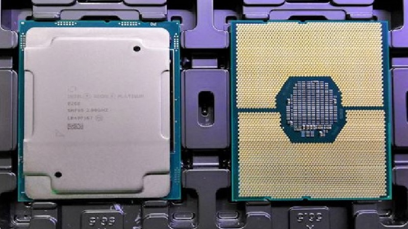
Ideally designed for the processors of the scalable server class, the Cooper Lake processors are branded as Xeon Gold and Xeon Platinum by Intel.
General information
- Transistors – 14 nm Tri-Gate
- Architecture – x86-64
- Cores – 16 to 28
- Socket – LGA 4189
- Predecessor – Cascade Lake
- Successor – Ice Lake processors of the same generation built on a 10 nm manufacturing process and targeted for 1S and 2S systems and next generation Sapphire Rapids.
Features
The features of the microarchitecture of Cooper Lake processors are mostly similar to those of the Skylake processors.
It has a faster memory, 2nd generation Optane memory support, and UPI links.
The most significant aspect of the Cooper Lake is that it is the first x86 processor that supports the bfloat16 instruction set.
It is a part of Deep Learning Boost of Intel.
However, it has some significant changes made to the architecture in comparison to its predecessor, Cascade Lake, such as:
- Six UPI or Ultra Path Interconnect links instead of three
- An improved memory with a higher data rate of up to 3200 MT/s instead of 2933 MT/s
- Optane DC DIMM support
- Barlow Pass support instead of Apache Pass
- Cedar Island bridge platform instead of Purley
- Socket-P+ flip-chip Land Grid Array or LGA with 4189 contacts instead of 3647 contacts
- A couple of new instructions such as Brian Float 16.
Enhancements
There are some notable enhancements made in the Cooper Lake processors which include:
- A new b-float16 instruction
- DDR4 memory support for up to 12 DIMMs per CPU socket
- -H: up to 1.12 TB of DDR4 per socket
- -HL: large Double Data Rate memory tier supports up to 4.5 TB.
Number of sockets
The Cooper Lake processors come with a varying number of sockets depending on their type, such as:
- The Xeon Platinum processors provide support for up to 8 sockets
- The Xeon Gold processors support up to four sockets
- The Xeon Silver and Bronze processors offer support for up to two sockets.
Pipeline
The Cooper Lake processors support superscalar pipelining with the following features included in them:
- Out of Order Execution (OoOE)
- Speculative execution
- Register renaming
There can be 14 to 19 stages involved in the pipeline.
Cache
The cache memory subsystem of the Cooper Lake processor has three levels with the Level 1 cache of 64 KB per core consisting of two types – half of it for the instructions and the other half for the data. It is summarized for you as follows:
Level 1 instruction cache:
- 32 KiB per core
- 8-way set associative
Level 1 data cache:
- 32 KiB per core
- 8-way set associative
- 1 MiB per core
- 16-way set associative
- 1.375 MiB per core
- 11-way set associative
Instruction Set Architecture and Extensions
The Cooper Lake processor supports x86-64 Instruction Set Architecture or ISA along with the following extensions:
- AES-NI or Advanced Encryption Standard New Instructions
- CLMUL or Carry-less Multiplication
- RDRAND or Read Random
- TXT or Text File extension
- FSGSBASE instructions for FS and GS segment registers
- MOVBE or Move Data After Swapping Bytes
- F16C or 16-bit Floating-Point conversion instructions
- BMI or Bit Manipulation Instructions along with BMI2
- RDSEED or Read Random SEED
- ADCX or Add-Carry Instruction Extensions
- PREFETCHW or Prefetch Data into Caches in Anticipation of a Write
- CLFLUSHOPT or Flush Cache Line Optimized
- XSAVE or Save Processor Extended States
- MPX or Memory Protection Extensions
- bfloat16 or Brain Float 16
- MMX or MultiMedia eXtensions
- SSE or Streaming SIMD Extensions, along with all its variants such as SSE2, SSE3, SSSE3, SSE4, SSE4.1,and SSE4.2
- AVX or Advanced Vector Extensions, along with AVX2 and AVX-512
- FMA3 or Fused Multiply Add
- TSX or Transactional Synchronization Extensions
- VT-x and VT-d or Virtualization extensions
Cooper Lake vs Ice Lake
- The Intel Cooper Lake processors are designed to meet the demands of the 4S and 8S multiprocessing market segments. On the other hand, the Intel Ice Lake processors are designed to serve the single-socket and dual-socket market sectors.
- The Cooper Lake processors are built on the 14 nm manufacturing technology of Intel, but in comparison, the Intel Ice Lake CPUs are built on the 10 nm technology node of Intel.
- The Cooper Lake CPUs usually come with a much higher core count in comparison to the Ice Lake processors.
- The Cooper Lake processors typically support the Brain Float 16 instruction extensions that help with machine learning and other near-sensor computing tasks, while the Ice Lake processors do not.
- The per core performance of the Cooper Lake processors is not as high as that of the Ice Lake processors in comparison, in spite of the fact that the latter comes with a much lower core count than the former.
- The Cooper Lake processors come with a lower Level 1 and Level 3 cache in comparison to the regular Ice Lake processors. However, the Level 2 cache size of the former is greater than the latter.
- The brand names of the two processors are significantly different. While the brand name of the Cooper Lake processors is Intel Xeon, the brand names of the regular Ice Lake processors are usually Intel Core i3, Core i5, and Intel Core i7.
- The microarchitecture of the Cooper Lake processors is that of Skylake, but in comparison, the Ice Lake processors come with the Sunny Cove microarchitecture.
- The socket of the Cooper Lake processors is typically a Land Grid Array, or an LGA 489 type, but in comparison, the socket of the regular Ice Lake processor is a typical Ball Grid Array, or a BGA 1526.
Conclusion
So, coming to the end of this article, you now surely have gained some knowledge about the features, architectural aspects and functionality of the Cooper Lake processors from the house of Intel.
It is, in fact, quite a good processor to use for AI-based workloads, which will expedite the process quite significantly.