")
In This Article
What is nm (Nanometer)?
A nanometer or nm in short, refers to a metric unit of structural measurement. It actually means a billionth of one meter. Mathematically it is represented as 10-9 or 1/1,000,000,000.
KEY TAKEAWAYS
- This unit of measurement is used in nanotechnology specifically to measure extremely small machine parts and electronics and computing parts in an atomic scale.
- The processors in the earlier days were large measuring about 32 nanometers but now these have shrunk to as small as 7 nanometers.
- Smaller the nm the better it is for a processor both in terms of cost and its performance.
Understanding nm (Nanometer) in Processor
Every processor is built using photolithography. This is the process in which the image of a processor is imprinted on a piece of silicon.
This technology of making a processor is normally called the process node or technology node.
This is usually to find out how small the transistors are made by the manufacturer.
The term ‘nm’ in the processor stands for Nanometer. This is actually a unit of measurement of length in a metric system.
It is the same as meters, centimeters, kilometers, but is miniscule as compared to those units. Ideally, nm is used to express the length in an atomic scale.
A comparison with the traditional metric system will make things much clearer to you. As you may know already, 1 kilometer is equal to 1000 meters and 1 meter is equal to 100 cm.
In that same measuring system, 1 cm is equal to 10000000 nm. Conversely, 1 nm is equal to 0.00000001 cm. To express this in words, it will be one billionth of a meter.
Therefore, you can see that 1 nm is a very small unit of measurement which is seldom used in daily life. (So, now you know why the sales reps avoid these terms.)
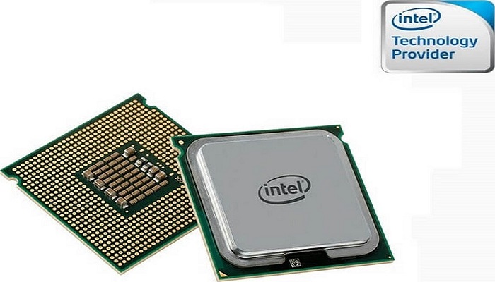
This measurement is typically used by the companies that use nanometer technology to measure the tiny products they make, such as TSMC or Taiwan Semiconductor Manufacturing Company, Intel, Samsung and more.
Technically speaking, nm in a processor is the measurement of the distance between the neighboring transistors in a processor design.
In fact, this measure gives a fair idea about how compact the transistors are.
These small processors are typically used in smartphones, tablets, laptops, and other smaller mobile devices.
It is said that a processor with lower nm is better but you should know the reason as well as the differences between them and the larger processors before you choose one instead of going with the crowd.
Well, the simple reason to say that the smaller processors are better is that the transistors in them are closer due to the compact size and therefore the electrons need to travel a shorter distance to perform a task. This offers significant benefits such as:
- Faster computing
- Less energy use
- Less heat dissipation and
- Lower thermal output across the board.
The smaller size of the die also increases the density as well as the cores in the chip.
Typically, nm refers to the lithography or fabrication process of the process.
As of now, Intel uses 10 nm or 14 nm technologies but TSMC typically uses the more compact 7 nm technology.
The processor manufacturing technology may differ from one company to another and so shall the nm in the processors.
However, different nanometers will offer different features.
Technically speaking, processors with different nm values will come with different transistor density.
It will be higher for the smaller nm processors. Typically, a 22 nm processor will have a transistor density of 16.5 MTr/mm² while a 14 nm processor will have a transistor density of 44.67 MTr/mm² and that of a 10 nm processor will be about 100 MTr/mm².
However, the value may vary a bit depending on the type of the processor, and of course, as said earlier, on the company.
Uses
Nm of processors is very important. Why? Well, for that you will need to look at things deeply and from a different perspective.
According to an old observation, Moore’s Law, the cost of transistors on a chip is halved but the number of them doubles every year.
This concept was true for quite some time but of late things started to change.
The size of the transistors started to be small in the late 1990s and early 2000s, almost to half of what it was before that time.
This resulted in huge improvements and the size shrunk further. This made things more complicated than offering more benefits.
Realizing this, several companies gave up the idea of reducing the size of their processors further.
For example, you would not see the Intel processors to have shrunk further since 2014.
However, other companies grabbed this opportunity with both hands and did the best to catch up with, and even surpass, Intel. Apple started producing its A12X chip with the 7 nm manufacturing process of TSMC and Samsung designed its own 10 nm chips.
Also, with AMD now taking on the 7 nm manufacturing technology, it has all the chances to eclipse Intel in terms of performance.
Therefore, nm is quite useful in processor manufacturing technology.
It not only helps them create a much better processor but also brings some healthy competition among the manufacturers.
It threatens the monopoly of Intel, no doubt.
Benefits
There are various benefits of designing or using a processor with lower nm lithography.
Some of these benefits are already mentioned above such as faster processing, low energy consumption and heat dissipation, and higher density of transistors.
Some of the other significant or allied benefits of a lower nm processor are mentioned below.
- Since the energy consumption will be low, heat dissipated will also be reduced by the processors. This means that you will not need to invest a huge amount of money in an outstanding cooling solution if you invest in a lower nm processor.
- The small die size will take up less space. This will allow making further architectural improvements.
- These chips usually have more cores available that will each act as a processor individually. This will result in higher frequency of the processor for a given budget and power as compared to the bulk.
- It will also result in exhibiting higher drive current than the planar devices per unit area and add to that there will also be a higher amount of on-chip cache.
Challenges
There are few challenges that are typically faced by the nm technology, and some of these challenges are quite significant.
First, there is an underlying issue with these silicon processors which is that the transistors are so close to each other.
This means that any further shrinking in size of the processors is quite impossible without a process called quantum tunneling coming into the picture.
This, however, creates another basic problem for the technology. It is that the transistors will not be shut off reliably due to the impact of it.
This is quite unfortunate and the worst part of it is that, in all probability and in most part, this issue will continue to exist.
Therefore, the manufacturers have to deal with the physical limitations of silicon that are real and extremely significant.
This will result in major difficulties while working with it if it is not taken well care of.
One significant way to deal with this issue is to keep a constant watch on the process curve as well as on the production process.
Also, the behavior of each of the factors is required to be tracked carefully. Often, the foundries find it very difficult to cope up with the other issues because they overlook this particular aspect.
There is another significant challenge in the form of the new process of patterning technology.
In today’s photolithography process, a light source with a wavelength of about 193 nm is used.
However, with a new technology available wherein EUV lithography is done with a light source with a wavelength of 13.5 nm, it presents the manufacturers with a net set of challenges.
It is assumed that the EUV or Extreme Ultraviolet can cause advanced chip scaling.
According to Moore’s law, it is perceived that the improvement of a microprocessor is rapid which is why the world has come to see laptops, smartphones, game consoles, and several other smart electronic devices within a few years time interval.
However, since mid-2016, the manufacturers realized that the cost of fabrication will be much higher due to the lower geometries of the chips.
This will make it quite impossible for them to meet the standards in terms of reliability in the processor and process parameters and at the same time meet the yield number.
Along with the developed manufacturing process, another significant challenge that the manufacturers face is the complexity in managing capacitance and resistance.
At the device level there are several local interconnects which can be achieved by middle-of-line process but it is the global interconnects that matter most.
These are typically done by the back-end-of-line and they are quite used to resistance-capacitance delays.
This is because at the lower nodes usually the back-end-of-line uses a multi-patterning process.
This results in delay as well as increases the cost of production due to additional etching and deposition in every pattern.
Since the industry is inclined to use extreme ultraviolet lithography for the lower process nodes, the back-end-of-line process can be expedited since the entire task will be done in one single exposure and the output can be tremendous.
Then there is also the challenge of the semiconductor design and manufacturing units.
According to the standard architecture these are supposed to work reliably but the yield has to be big in order to be profitable.
Conclusion
Therefore, as this article points out, the smaller nm of the processor is good both in terms of performance and cost.
Now that you know quite a lot about the nm technology, it will be much easier for you to make a choice.