
There are different types of SIMMs or Single In-line Memory Modules that come with different types of pin configurations based on which they are categorized.
Most users know that there are 30-pin SIMMs and 72-pin SIMMs but those are not the only ones. Also, they are not aware of the pin configurations.
This particular article will clear all confusions and will also make you knowledgeable about the pins and how each of them is described without you needing to go through a multiple of websites for it.
In This Article
KEY TAKEAWAYS
- There are usually 30-pin, 72-pin and GVP 64-pin Single Inline Memory Modules available in the market.
- Whether it is a 30-pin SIMM or a 72-pin SIMM or any other, the configurations and purposes of each vary.
- Just like the look, their sizes may even vary and some may be single-sided while others may be double-sided or both.
What Are the Types of SIMMs and Their Pin Configurations?
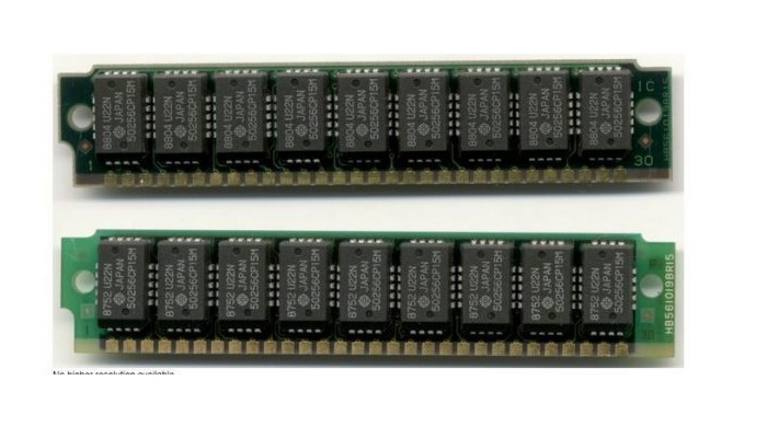
As already mentioned before there are two types of Single In-line Memory Modules available and it is typically categorized by the number of pins present in them.
One of its variants comes with 30 pins and the other has as many as 72 pins in it.
Apart from that, you will also get a few specific types of proprietary SIMMs as follows with specific features such as:
The GVP 64-pin SIMMs – These Great Valley Products for the Commodore Amiga comes with 64 pins and other features such as:
- 32 bits width
- 1 MB, 4 MB or and 16 MB size and
- 60 ns access time.
The Apple 64-pin SIMMs – These Apple products are dual-ported and are used in Apple Macintosh II FX computers.
These SIMMs came with specific features such as:
- Overlapping read and write cycles
- 1 MB, 4 MB, 8 MB, and 16 MB size and
- 80 ns access time.
In addition to the differences in pins, you will also get the SIMMs in two particular styles namely:
- Single-sided SIMMs and
- Double-sided SIMMs.
This actually means whether the Dynamic RAM chips are found only on one side of the SIMM or on both sides of it.
Typically, all 30-pin SIMMs are single-sided but the 72-pin SIMMs can be both, single-sided or double-sided.
However, there are a few specific types of double-sided SIMMs that are built as composite SIMMs.
Usually, those SIMMs that come with 32 chips on them are composite SIMMs, almost always.
Typically, these variants are wired internally and look like two single-sided SIMMs actually wired back to back.
This, however, did not change the number of data bits that they could transmit in each clock cycle or the number of it you want to use.
Moreover, there are a few specific types of motherboards that cannot handle the composite SIMMs since these are a little bit different electrically.
However, the 72-pin SIMMs with a capacity of 1 MB, 4 MB and 16 MB are usually single-sided.
On the other hand, those with a capacity of 2 MB, 8 MB and 32 MB are usually double-sided.
It is for this reason you will find different motherboards that will support only 1 MB, 4 MB and 16 MB Single in-line Memory Modules.
Therefore, you should always check the motherboard you want to buy or use so that it supports the right size and type of SIMM for your type of computing jobs.
Usually, if a motherboard does not support a composite SIMM, it will not work.
How Many Pins SIMM Have?
As said earlier, the SIMMs typically come with either 30 pins or 72 pins.
Here is a brief description of each of these two types of Single In-line Memory Modules.
30-pin SIMMs:
The 30-pin memory modules usually come in a variety of sizes such as:
- 256 KB
- 1 MB
- 4 MB and
- 16 MB.
There are 12 address lines available in the 30-pin SIMMs that can provide as many as 24 address bits in total.
This means that using an 8 bit data width, it will result in a highest capacity of 16 MB.
However, at this point it should be remembered that the extra redundancy bit chip does not normally contribute to the capacity that can be used.
This is applicable for parity as well as the non-parity modules both though the pins 26, 28 and 29 on the non-parity SIMMs are typically not connected.
Here are the distinct names and signal descriptions of each of all of the 30 pins in a 30-pin SIMM:
- Pin 1 is named VCC and its signal is described as +5 VDC
- Pin 2 is named /CAS and its signal is described as Column Address Strobe
- Pin 3 is named DQ0 and its signal is described as Data 0
- Pin 4 is named A0 and its signal is described as Address 0
- Pin 5 is named A1 and its signal is described as Address 1
- Pin 6 is named DQ1 and its signal is described as Data 1
- Pin 7 is named A2 and its signal is described as Address 2
- Pin 8 is named A3 and its signal is described as Address 3
- Pin 9 is named VSS and its signal is described as Ground
- Pin 10 is named DQ2 and its signal is described as Data 2
- Pin 11 is named A4 and its signal is described as Address 4
- Pin 12 is named A5 and its signal is described as Address 5
- Pin 13 is named DQ3 and its signal is described as Data 3
- Pin 14 is named A6 and its signal is described as Address 6
- Pin 15 is named A7 and its signal is described as Address 7
- Pin 16 is named DQ4 and its signal is described as Data 4
- Pin 17 is named A8 and its signal is described as Address 8
- Pin 18 is named A9 and its signal is described as Address 9
- Pin 19 is named A10 and its signal is described as Address 10
- Pin 20 is named DQ5 and its signal is described as Data 5
- Pin 21 is named /WE and its signal is described as Write Enable
- Pin 22 is named VSS and its signal is described as Ground
- Pin 23 is named DQ6 and its signal is described as Data 6
- Pin 24 is named A11 and its signal is described as Address 11
- Pin 25 is named DQ7 and its signal is described as Data 7
- Pin 26 is named QP and its signal is described as Data parity out and is not connected on non-parity SIMMs
- Pin 27 is named /RAS and its signal is described as Row Address Strobe
- Pin 28 is named /CASP and its signal is described as Parity Column Address Strobe and is not connected on non-parity SIMMs
- Pin 29 is named DP and its signal is described as Data parity in and is not connected on non-parity SIMMs and
- Pin 30 is named as VCC and its signal is described as +5 VDC.
72-pin SIMMs:
The standard sizes of the 72-pin SIMMs are however much wider and varied which include:
- 1 MB
- 2 MB
- 4 MB
- 8 MB
- 16 MB
- 32 MB
- 64 MB and
- 128 MB.
This standard is also followed for the 3.3 volt modules that come with further address lines and up to 2 GB.
In this particular type of memory modules there are 12 address lines that offer a maximum of 24 address bits, 32 bit data output, dual ranks of chips, and an absolute maximum capacity of 128 MB.
On the non-parity SIMMs the 35, 36, 37 and 38 pins are not connected.
Here are the distinct names and signal descriptions of each of all of the 72 pins in a 5 volt 72-pin SIMM:
- Pin 1 is named VSS and its signal is described as Ground
- Pin 2 is named MD0 and its signal is described as Data 0
- Pin 3 is named MD16 and its signal is described as Data 16
- Pin 4 is named MD1 and its signal is described as Data 1
- Pin 5 is named MD17 and its signal is described as Data 17
- Pin 6 is named MD2 and its signal is described as Data 2
- Pin 7 is named MD18 and its signal is described as Data 18
- Pin 8 is named MD3 and its signal is described as Data 3
- Pin 9 is named MD19 and its signal is described as Data 19
- Pin 10 is named VCC and its signal is described as +5 VDC
- Pin 11 is named NU [PD5] and its signal is described as Not Used [Presence Detect 5 (3v3)] which means these lines are defined only in 3.3 volt memory modules
- Pin 12 is named MA0 and its signal is described as Address 0
- Pin 13 is named MA1 and its signal is described as Address 1
- Pin 14 is named MA2 and its signal is described as Address 2
- Pin 15 is named MA3 and its signal is described as Address 3
- Pin 16 is named MA4 and its signal is described as Address 4
- Pin 17 is named MA5 and its signal is described as Address 5
- Pin 18 is named MA6 and its signal is described as Address 6
- Pin 19 is named MA10 and its signal is described as Address 10
- Pin 20 is named MD4 and its signal is described as Data 4
- Pin 21 is named MD20 and its signal is described as Data 20
- Pin 22 is named MD5 and its signal is described as Data 5
- Pin 23 is named MD21 and its signal is described as Data 21
- Pin 24 is named MD6 and its signal is described as Data 6
- Pin 25 is named MD22 and its signal is described as Data 22
- Pin 26 is named MD7 and its signal is described as Data 7
- Pin 27 is named MD23 and its signal is described as Data 23
- Pin 28 is named MA7 and its signal is described as Address 7
- Pin 29 is named MA11 and its signal is described as Address 11
- Pin 30 is named VCC and its signal is described as +5 VDC
- Pin 31 is named MA8 and its signal is described as Address 8
- Pin 32 is named MA9 and its signal is described as Address 9
- Pin 33 is named /RAS3 and its signal is described as Row Address Strobe 3 and is only used in two ranked SIMMs with 2 MB, 8 MB, 32 MB, and 128 MB sizes
- Pin 34 is named /RAS2 and its signal is described as Row Address Strobe 2
- Pin 35 is named MDP2 and its signal is described as Data Parity 2 (MD16…23) and is not connected on non-parity SIMMs
- Pin 36 is named MDP0 and its signal is described as Data Parity 0 (MD0…7) and is not connected on non-parity SIMMs
- Pin 37 is named MDP1 and its signal is described as Data Parity 1 (MD8…15) and is not connected on non-parity SIMMs
- Pin 38 is named MDP3 and its signal is described as Data Parity 3 (MD24…31) and is not connected on non-parity SIMMs
- Pin 39 is name VSS and its signal is described as Ground
- Pin 40 is named /CAS0 and its signal is described as Column Address Strobe 0
- Pin 41 is named /CAS2 and its signal is described as Column Address Strobe 2
- Pin 42 is named /CAS3 and its signal is described as Column Address Strobe 3
- Pin 43 is named /CAS1 and its signal is described as Column Address Strobe 1
- Pin 44 is named /RAS0 and its signal is described as Row Address Strobe 0
- Pin 45 is named /RAS1 and its signal is described as Row Address Strobe 1 and is only used in two raked SIMMs with 2 MB, 8 MB, 32 MB, and 128 MB sizes
- Pin 46 is named NC and its signal is described as Not Connected
- Pin 47 is named /WE and its signal is described as Read/Write Enable
- Pin 48 is named NC [/ECC] and its signal is described as Not Connected [ECC presence if grounded (3v3)] which means these lines are defined only in 3.3 volt memory modules
- Pin 49 is named MD8 and its signal is described as Data 8
- Pin 50 is named MD24 and its signal is described as Data 24
- Pin 51 is named MD9 and its signal is described as Data 9
- Pin 52 is named MD25 and its signal is described as Data 25
- Pin 53 is named MD10 and its signal is described as Data 10
- Pin 54 is named MD26 and its signal is described as Data 26
- Pin 55 is named MD11 and its signal is described as Data 11
- Pin 56 is named MD27 and its signal is described as Data 27
- Pin 57 is named MD12 and its signal is described as Data 12
- Pin 58 is named MD28 and its signal is described as Data 28
- Pin 59 is named VCC and its signal is described as +5 VDC
- Pin 60 is named MD29 and its signal is described as Data 29
- Pin 61 is named MD13 and its signal is described as Data 13
- Pin 62 is named MD30 and its signal is described as Data 30
- Pin 63 is named MD14 and its signal is described as Data 14
- Pin 64 is named MD31 and its signal is described as Data 31
- Pin 65 is named MD15 and its signal is described as Data 15
- Pin 66 is named NC [/EDO] and its signal is described as Not Connected [EDO presence (if grounded) (3v3)] which means that these lines are defined only for 3.3 volt memory modules
- Pin 67 is named PD1 and its signal is described as Presence Detect 1 according to the JEDEC Standard
- Pin 68 is named PD2 and its signal is described as Presence Detect 2 according to the JEDEC Standard
- Pin 69 is named PD3 and its signal is described as Presence Detect 3 according to the JEDEC Standard
- Pin 70 is named PD4 and its signal is described as Presence Detect 4 according to the JEDEC Standard
- Pin 71 is named NC [PD (ref)] and its signal is described as Not Connected [Presence Detect (ref) (3v3)] which means that these lined are defined only for 3.3 memory modules
- Pin 72 is named VSS and its signal is described as Ground.
The GVP and Apple 64-pin proprietary SIMMs however have a little different pin configuration as under:
- Pin 1 is named GND and its signal is described as Ground
- Pin 2 is named NC and its signal is described as Not connected
- Pin 3 is named +5V and its signal is described as +5 volts
- Pin 4 is named +5V and its signal is described as +5 volts
- Pin 5 is named /CAS and its signal is described as Column address strobe
- Pin 6 is named D0 and its signal is described as Data input bus, bit 0
- Pin 7 is named Q0 and its signal is described as Data output bus, bit 0
- Pin 8 is named /W0 and its signal is described as Write-enable input for RAM IC 0
- Pin 9 is named A0 and its signal is described as Address bus, bit 0
- Pin 10 is named NC and its signal is described as Not connected
- Pin 11 is named A1 and its signal is described as Address bus, bit 1
- Pin 12 is named D1 and its signal is described as Data input bus, bit 1
- Pin 13 is named Q1 and its signal is described as Data output bus, bit 1
- Pin 14 is named /W1 and its signal is described as Write-enable input for RAM IC 1
- Pin 15 is named A2 and its signal is described as Address bus, bit 2
- Pin 16 is named NC and its signal is described as Not connected
- Pin 17 is named A3 and its signal is described as Address bus, bit 3
- Pin 18 is named GND and its signal is described as Ground
- Pin 19 is named GND and its signal is described as Ground
- Pin 20 is named D2 and its signal is described as Data input bus, bit 2
- Pin 21 is named Q2 and its signal is described as Data output bus, bit 2
- Pin 22 is named /W2 and its signal is described as Write-enable input for RAM IC 2
- Pin 23 is named A4 and its signal is described as Address bus, bit 4
- Pin 24 is named NC and its signal is described as Not connected
- Pin 25 is named A5 and its signal is described as Address bus, bit 5
- Pin 26 is named D3 and its signal is described as Data input bus, bit 3
- Pin 27 is named Q3 and its signal is described as Data output bus, bit 3
- Pin 28 is named /W3 and its signal is described as Write-enable input for RAM IC 3
- Pin 29 is named A6 and its signal is described as Address bus, bit 6
- Pin 30 is named NC and its signal is described as Not connected
- Pin 31 is named A7 and its signal is described as Address bus, bit 7
- Pin 32 is named D4 and its signal is described as Data input bus, bit 4
- Pin 33 is named as Q4 and its signal is described as Data output bus, bit 4
- Pin 34 is named /W4 and its signal is described as Write-enable input for RAM IC 4
- Pin 35 is named A8 and its signal is described as Address bus, bit 8
- Pin 36 is named NC and its signal is described as Not connected
- Pin 37 is named A9 and its signal is described as Address bus, bit 9
- Pin 38 is named A10 and its signal is described as Address bus, bit 10
- Pin 39 is named A11 and its signal is described as Address bus, bit 11
- Pin 40 is named D5 and its signal is described as Data input bus, bit 5
- Pin 41 is named Q5 and its signal is described as Data output bus, bit 5
- Pin 42 is named /W5 and its signal is described as Write-enable input for RAM IC 5
- Pin 43 is named NC and its signal is described as Not connected
- Pin 44 is named NC and its signal is described as Not connected
- Pin 45 is named GND and its signal is described as Ground
- Pin 46 is named D6 and its signal is described as Data input bus, bit 6
- Pin 47 is named Q6 and its signal is described as Data output bus, bit 6
- Pin 48 is named /W6 and its signal is described as Write-enable input for RAM IC 6
- Pin 49 is named NC and its signal is described as Not connected
- Pin 50 is named D7 and its signal is described as Data input bus, bit 7
- Pin 51 is named Q7 and its signal is described as Data output bus, bit 7
- Pin 52 is named /W7 and its signal is described as Write-enable input for RAM IC 7
- Pin 53 is named /QB and its signal is described as Reserved parity
- Pin 54 is named NC and its signal is described as Not connected
- Pin 55 is named /RAS and its signal is described as Row address strobe
- Pin 56 is named NC and its signal is described as Not connected
- Pin 57 is named NC and its signal is described as Not connected
- Pin 58 is named Q and its signal is described as Parity-check output
- Pin 59 is named /WWP and its signal is described as Write wrong parity
- Pin 60 is named PDCI and its signal is described as Parity daisy-chain input
- Pin 61 is named +5V and its signal is described as +5 volts
- Pin 62 is named +5V and its signal is described as +5 volts
- Pin 63 is named PDCO and its signal is described as Parity daisy-chain output
- Pin 64 is named GND and its signal is described as Ground.
You will also get the HP LaserJet Single In-line Memory Modules with 72 pins and with non-standard PD or Presence Detect connections.
Conclusion
So, coming to the end of this article, now you are surely quite educated about the types of Single Inline Memory Modules you get in the market along with the diverse purposes of the pins they have.
Now you also know how complex the working process of a SIMM is with each pin working differently.