")
In This Article
What is BGA (Ball Grid Array)?
Ball Grid Array, or BGA, refers to a memory chip with small solder balls fixed on the bottom for mounting. In simple words, the BGA does not have pins like the PGA or Pin Grade Array.
Technically, BGA follows a specific type of Surface Mount Technology or SMT in which the connectors are solder balls set underneath the chip made up of ceramic or plastic in the form of a grid.
KEY TAKEAWAYS
- The design of Ball Grid Array is based on Pin Grade Array technology with the difference that in place of the pins, small solder balls are used for connectivity.
- The BGA packages allow high-density connectivity with low-voltage usage with the Integrated Circuits.
- The backside of the compact BGAs is connected through different sockets such as Y contact sockets, spring contact sockets, side contact sockets, tweezers contact sockets and more.
- These chips come in different form factors and a specific package can be identified easily by the number of sockets present in it.
- There are different types of BGAs available such as the plastic molded type, the flex tape type, high thermal metal top type with low profiles and more.
Understanding BGA (Ball Grid Array)
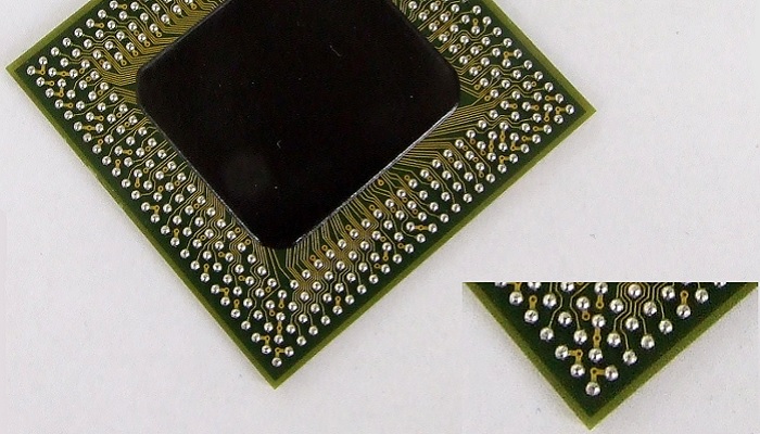
Ball Grid Array is derived from the PGA or Pin Grid Array technology. The solder balls used in its design conduct the electrical signals from one IC to another on the PCB through conductive printed wires.
The BGA chip can normally come in the most common green color but these are also available in different colors such as:
- Red
- Black
- Blue or
- White.
All of the components of the chip are packed electronically into a standard package.
The underside of the silicon die interposer offers connectivity with different types of sockets such as:
- Y contact sockets
- Tweezers contact sockets
- Spring contact sockets
- Side contact sockets
- Metal dendrite contacts and
- Wire in elastomer contacts.
BGA has paved the way to CSP or Chip Scale Packaging which is not larger than 1.2x the size of the semiconductor die itself.
Apart from a compact size, the other significant benefits that a BGA offers are:
- A high lead count and a high density
- A low inductance
- A low voltage usage
- Low thermals as heat can be routed through the pads and
- Easy alignment of the chip with the Printed Circuit Board.
The best part of BGA is that there is little to no chance of bridging them together while soldering as there is with PGA pins. This is because the solder balls are placed evenly apart.
However, there are some downsides of BGAs including:
- Possibilities of issues as result of the thermal expansion due to their non-mechanical compliance
- Significant difficulty in finding out the defects in soldering when the BGA is placed on the Printed Circuit Board and
- Unique and costly equipment is required because manual soldering is complicated and untrustworthy for these packages.
The BGA packages are available in different packages and form factors and are easily identified by the number of sockets in each.
For example, if it is a BGA 437 package, it will typically come with 437 sockets and a BGA 441 package will have 441 sockets in it.
BGA Package Types
The Ball Grid Arrays are available in a wide range of types which include PBGAs, TBGAs, HL-PBGAs, and H-PBGAs, to name a few. All these different types meet the diverse needs of the different types of equipment and assembly.
MAPBGA:
The Molded Array Process Ball Grid Array package is designed to be used in low to mid range performance devices offering ease in surface mounting and low inductance. In spite of being a low-cost option PBGAs offer a high level of reliability and a small footprint.
PBGA:
The Plastic Ball Grid Array package is also designed to be used in mid and low range devices offering low inductance and ease in mounting.
It offers a high level of reliability, low cost and comes with extra layers of copper in the substrate. This helps in handling higher power dissipation levels.
TEPBGA:
The Thermally Enhanced Plastic Ball Grid Array package is designed with thicker copper planes in its substrate. This helps handle much higher levels of heat dissipation needs by drawing more heat to the board from the die.
TBGA:
The Tape Ball Grid Array or Thin BGA package is particularly designed for use in a mid-range to high-end solution and for applications that require high thermal performance. There is no need for an external heat sink.
PoP:
Package on Package is a special type of BGA that can be used in those particular applications where space is a real concern. The best part is that it allows stacking a memory package on top of the base device.
Micro BGA:
Just as the name signifies, Micro BGA is a package which is much smaller in size as compared to the regular BGA package.
In addition to the above types, there are also several different versions of BGA packages available. In chronological order, these are:
- CABGA – Chip Array Ball Grid Array
- CTBGA – Thin Chip Array Ball Grid Array
- CVBGA – Very Thin Chip Array Ball Grid Array
- DSBGA – Die-Size Ball Grid Array
- FBGA – Fine Ball Grid Array Also Known As Fine Pitch Ball Grid Array
- FCmBGA – Flip Chip Molded Ball Grid Array
- LBGA – Low-profile Ball Grid Array
- LFBGA – Low-profile Fine-pitch Ball Grid Array
- MBGA – Micro Ball Grid Array
- MCM – PBGA: Multi-Chip Module Plastic Ball Grid Array
- nFBGA – New Fine Ball Grid Array
- SuperBGA or SBGA – Super Ball Grid Array
- TABGA – Tape Array BGA
- TFBGA – Thin And Fine Ball Grid Array
- UFBGA or UBGA – Ultra Fine Ball Grid Array
- VFBGA – Very Fine Pitch Ball Grid Array and
- WFBGA – Very Thin Profile Fine Pitch Ball Grid Array.
There is also an Intel Mobile Celeron in a flip-chip BGA 2 package called FCBGA-479. This die is dark blue in color and is mounted to a PCB substrate under it using an underfill and flip chip.
It is called the interposer and is usually dark yellow in color. There is an NVIDIA GeForce 256 GPU inside this wire-bond BGA package.
How Does a BGA Work?
Typically, it is the solder balls that connect the array with the PCB and it contains a controlled amount of solder to make it work.
- The system raises the levels of integration to unparalleled levels to meet the needs of the Integrated Circuits
- The huge number of pins and gates controls the flow of electric signals and
- The controlled reflow soldering technique prevents accidental bridging of the connectors.
What is a BGA Socket?
A BGA socket refers to an electromechanical device. This actually offers a removable interface between the circuit board of the system and the Integrated Circuit package. It also ensures there is minimal or no signal integrity during removal.
Different types of other technologies are also used in the BGA socket design such as:
SG Elastomer:
These sockets are usually built for prototype applications and use low-cost elastomer contact technology, silicon validation and development. There is a shoulder screw in the socket along with a swivel lid.
This allows a quick insertion so that the IC can be changed quickly. The socket has a small footprint of 2.5 mm on each side and is mounted on the printed board without soldering.
Torque Tool:
Sometimes, a torque tool may be integrated into a BGA socket as an alternative option. This allows applying vertical force through the compression screw. It also enhances the life, repeatability, and reliability of the elastomer contacts.
GT Elastomer:
Almost similar to the SG elastomer contact technology, GT elastomer BGA sockets offer a bandwidth of 94 GHz, lower self and mutual inductance, lower mutual capacitance and contact resistance.
Stamped Spring Pin:
The Stamped Spring Pin or SBT contact technology is also used in many BGA sockets that can be mounted on as GT or SG BGA sockets.
These are low-cost sockets that offer better mechanical and electrical performance than traditional pin sockets. The outside spring and the inside leaf spring offer a strong solution for test and burn-in applications.
There are also different types of BGA sockets available based on the varied technologies such as:
With thermal access hole:
These holes serve two purposes such as for pacing a thermocouple from the top and accessing the BGA’s case temperature and also to use a thermal chamber to force hot air through the top which escapes through the compression plate of the socket.
With existing mounting holes:
These holes help using the BGA socket on PCBs made with top side components with the areas for the top side components cleared.
With two mounting holes only:
These particular BGA sockets built with SBT mounting technology allow more room to add components as well as route channels on the top layer for PCB traces.
SMP sockets:
These BGA sockets normally use silver ball matrix contact technology. There is a defensive plunger matrix which typically is a gold plated copper cylinder on top of the conductive column to prevent it from being contaminated by different solder ball interfaces because of the high cycle count.
With insulation plate:
All BGA socket designs include a stiffener or a back support plate to balance the vertical force needed to connect the chip to the spring pins or elastomer which in turn connects to the pads of the target PCB.
Since this applied force varies due to pitch, pin count, and contact technology used, in most cases, the backside of the board contains resistors and capacitors.
However, the stiffener cannot go above the components and so a custom insulation plate is used for the resistors and capacitors with cavities milled into it and is placed between the printed circuit board and the back support plate.
With backing plate:
An alternative solution to the above is a BGA socket with a 5 post backing plate. The locations of the posts are predetermined for the PCB as keep-out zones.
These back plates with post locations jutting out allow the resistors and capacitors to be populated in between them.
SMT adapter bases:
Adapter bases are also available on the BGA sockets when through-hole mounting is not likely on the target PCB to mount the sockets manually.
Emulating the footprint of the BGA, these bases change the socket into an SMT component so that it can be installed easily with reflow and standard flux and techniques.
When the SMT adapter bases are soldered down to the BGA pads on the board, the sockets can be easily mounted mechanically to them using hardware.
Stack up SMT adapters:
These are alternative solutions where larger SMT adapter bases than the IC device cannot be used due to the hardware on the sides and the four corners or when other passive parts are needed to be set nearby chip on the target PCB.
These solutions lift the adapter up to allow placing the components close by.
Epoxy-mounted sockets:
Both types of SMT adapters add signal length, which reduces signal speed, and is not desirable for testing applications. As an alternative solution, an epoxy-mounted BGA socket can be used.
It is designed to create a more or less permanent bonding to the PCB and the contacting components can be replaced if they are damaged due to excessive wear.
There is simply an epoxy band around the border on which the socket is mounted on the PCB.
How is BGA Made?
Ball Grid Array is made up of multiple insulating and conducting layers overlapping each other with a solder mask for packaging Integrated Circuits.
These overlapping layers are typically made up of thin copper foil measured usually in micrometers or ounces per square foot. The insulation material in the chip is usually dielectric.
These layers are bonded together normally with epoxy resin composite fibers called pre-preg.
In the BGA packages, an organic substrate is used in place of a lead frame. This substrate is usually made up of polyimide or bismaleimide triazine and the chip is mounted on top of it.
The solder balls at the underside of the substrate establish the connections to the printed circuit board.
What is BGA in an SSD?
The Ball Grid Array Solid State Drives are small but offer up 1500x higher performance than any regular HDD. It is a significant innovation in personal computing.
The design of these SSDs makes them so useful which includes:
- A dense 3D Vertical NAND technology with semiconductor sells
- Dynamic RAM memory
- A controller chip
- Five times smaller size than an M.2 SSD and 100 times smaller than a 2.5-inch memory
- Low weight
- Lower power consumption
- Higher cell endurance
- Higher numbers of bits per NAND cell
- Greater reliability
- Better thermal dissipation
- Vibration and shock resistant, being soldered down
- PCIe interface and flash-optimized NVMe protocol
- High sequential read and write speeds of up to 1,500 Mbps and 900 MB/s
- Higher random read and write Input Output Operations Per Second or IOPS
- Better and seamless user experience and
- Compatibility with almost any notebook.
Using similar underlying software as the M.2 form factor, the BGA SSDs have no additional design requirements but can hold more data, last longer, work on any given and extreme conditions and perform reliably offering the best total cost of ownership.
How Do You Test a BGA?
The best way to test for BGA failure is by performing a dye and pry test. This test is destructive but cost-effective.
The steps to follow are:
- Remove the area of the board containing the target part by using a diamond saw blade
- Immerse it in a low-viscosity red dye inside a vacuum chamber
- Bake it in a moisture-removal oven till it is dry
- Use a puller assembly to separate the part from the board and
- Check under a microscope to see where the dye has penetrated the component to indicate a defect.
What is BGA Assembly?
BGA assembly refers to the process of mounting BGAs using the solder reflow process on the PCB. It offers reliable connectivity. This assembly is heated during the soldering process, which melts the solder.
The solder balls are usually heated after being placed on the underside of the BGA package in a grid layout.
These balls are melted in a reflow oven. Surface tension is used to align the package with the PCB.
When the balls cool, they solidify with a consistent and accurate distance between them.
This offers several benefits such as:
- Improved thermal and electrical performance
- Reduced board thickness
- Lower chances of PCB damage
- Usability in small packages with high pin count
- Faster assembly process
- Improved solderability and
- Quick heat dissipation.
BGA Vs LGA
- The BGA is much smaller in size in comparison to the LGA package
- BGA is typically used in CPUs for notebooks and smartphones while LGA is usually used in desktop CPUs
- The one-time BGA package has no visible pins on the outside but the contacts of LGA are on the PCB of the CPU and the pins are on the motherboard
- The BGA package cannot be replaced easily and separately without using processional tools as opposed to an LGA package
- A BGA package has a very small thermal conductivity in general as opposed to the LGA package which has a higher thermal conductivity due to its larger size and bulk
- Power consumption in BGA is lower in comparison to an LGA package due to its smaller size and
- BGA uses balls at the underside to connect to the motherboard but LGAs use pins for that matter.
BGA Pin Numbering Standard
The pins in the Ball Grid Array usually use a number for X and a letter for Y. Typically, a few numbers that look similar such as I, O, Q, S, X, and Z are not used. Therefore, a regular pin configuration standard for a large BGA would be AJ22, AP15, C4, K9, and others.
Questions & Answers:
Can You Upgrade a BGA CPU?
If you have a laptop computer and it has a BGA socket, then such upgrades are not possible. If the processor was not soldered, it could have been upgraded but for that, the processor has to be BIOS, chipset and socket compatible.
Is BGA Flip Chip?
A BGA can be a flip chip which comes with a special kind of Ball Grid Array that allows for a controlled, collapse chip connection.
There are solder bumps on the surface of the chip pads and Integrated Circuits on the wafer. The solder balls are fixed to each of the pads that are metalized on the chip.
Where is BGA Used?
A Ball Grid Array is typically used for Integrated Circuits and in devices such as microprocessors, in DIMM or flat packages, and several electronic products such as Wi-Fi chips, FPGAs, computer chipsets, RAM devices, and microcontrollers.
What is BGA Ball Pitch?
BGA Ball pitch refers to the distance between the center of one solder ball to that of the next one. There are typically three pitches widespread in the industry such as 0.65 mm, 0.75 mm and 0.8 mm.
However, the Micro BGAs used in almost every smartphone come with a 0.3 mm ball pitch and while the ultra-fine BGAs used in next generation products come with a 0.2 mm ball pitch.
Conclusion
The Ball Grid Arrays offer a reliable connectivity with their unique design, where solder balls are used.
In this chip, there are one to a million logic gates, multiplexers, flip-flops and other circuits.
It is commonly used in smaller devices and several other computer products.